


Our journal "Nanosystems: Physics, Chemistry, Mathematics" is devoted to fundamental problems of physics, chemistry and mathematics concerning all aspects of nanosystems science. It considers both theoretical and experimental problems of physics and chemistry of nanosystems, including methods of their design and creation, studies of their structure and properties, behavior under external influences, and the possibility of use. We accept papers directly or conceptually related to the key properties of nanosystems. Nanotechnology has required the creation of new methods of mathematical modeling and mathematical physics, as well as the development of existing methods for their extension to the study of new objects, many of which were previously simply absent. The corresponding mathematical problems will be covered in our journal. The scope of the journal includes all areas of nano-sciences. Papers devoted to basic problems of physics, chemistry and mathematics inspired by nanosystems investigations are welcomed. Both theoretical and experimental works concerning the properties and behavior of nanosystems, problems of their creation and application, mathematical methods of nanosystem studies are considered. The journal publishes scientific reviews (up to 30 journal pages), research papers (up to 15 pages) and letters (up to 5 pages). All manuscripts are peer-reviewed. Authors are informed about the referee opinions and the Editorial decisions.
Current issue
MATHEMATICS

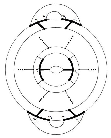
We investigate translation-invariant Gibbs measures of the Hard-Core–Potts (HC–Potts) model on the Cayley tree. The model combines Potts-type ferromagnetic interactions with a hard-core exclusion rule, leading to a nontrivial interplay between magnetic ordering and occupancy constraints. For the hinge-type fertile graph, we analyze the cases k = 2 and k = 3, and determine explicit critical values of θ that mark the transition from uniqueness to multiplicity of Gibbs measures. The model exhibits up to five translationinvariant phases depending on the interaction strength. Thermodynamic quantities such as magnetization and quadrupolar moment are computed, revealing ordered phases at low temperatures and a paramagnetic phase at high temperatures.
A perfect star packing can be described as a spanning subgraph whose connected components are isomorphic to the star graph K1,3. A perfect pseudo-matching is a spanning subgraph in which every component is isomorphic to either K2 or K1,3. The study of packing problems on fullerene graphs is of particular interest due to their potential relevance in describing local bonding arrangements in carbon nanostructures. In this paper, we study the uniqueness of perfect star packing, and the existence of pseudo-matchings in (2, 6)- fullerene graphs. Moreover, we show that the perfect star packing in these graphs is unique. Furthermore, we introduced some perfect pseudo-matchings in (2, 6)-fullerene graphs.
In this paper, Gibbs measures of the Hard-Core-Potts model on the Cayley tree are studied. The model unifies magnetic ordering and exclusion effects, providing a framework for describing phase transitions. For the hinge-type graph, the cases $k = 2$ and $k = 3$ are analyzed, and the corresponding critical parameters are determined. Thermodynamic analysis shows that the system exhibits ordered (ferromagnetic) phases at low temperatures and disordered (paramagnetic) phases at high temperatures. The results reveal the interrelation between magnetic and structural phase transitions.
A perfect star packing can be described as a spanning subgraph whose connected components are isomorphic to the star graph K1;3. A perfect pseudo-matching is a spanning subgraph in which every component is isomorphic to either K2 or K1;3. The study of packing problems on fullerene graphs is of particular interest due to their potential relevance in describing local bonding arrangements in carbon nanostructures. In this paper, we study the uniqueness of perfect star packing, and the existence of pseudo matchings in (2; 6)-fullerene graphs. Moreover, we show that the perfect star
packing in these graphs is unique. Furthermore, we introduced some perfect pseudo-matchings in (2; 6)-fullerene graphs.
PHYSICS
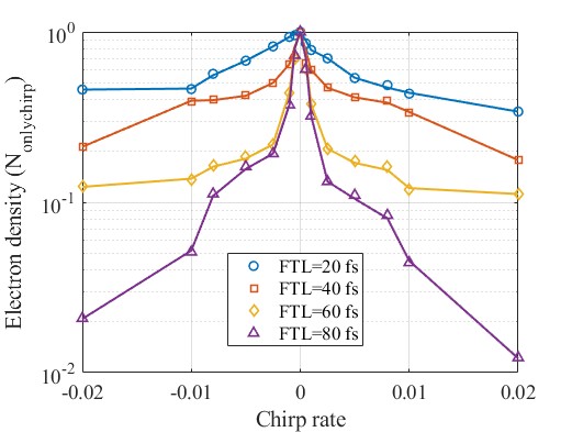
We present a theoretical study of how linear chirp controls plasma density in a water jet using a two-stage framework. Stage I solves carrier-population and current equations at a single point, driven by a chirped super-Gaussian pulse. By fixing bandwidth and normalizing for intensity, we isolate a chirp-only response of plasma density, which exceeds unity and shows a consistent advantage for negative over positive chirp. Stage II propagates the field in water via the angular-spectrum method and applies the same equations across space. Normal dispersion reverses the trend: the chirp-only plasma density decreases as chirp grows, negative chirp remains less detrimental, and suppression is strongest for longer FTL pulses (e.g., 80 fs) due to dispersion-induced temporal spreading and spatio-temporal desynchronization. This study separates spectralphase effects from bandwidth and intensity, yields testable predictions for water jets, and provides a foundation for future experiments and self-consistent propagation models.

This study explores the application of spin waves for developing functional components for information processing, transmission, and storage within the microwave and terahertz frequency regimes. The platform is based on yttrium iron garnet thin films, with spin wave manipulation achieved via two-dimensional arrays of magnetite cylinders. A numerical micromagnetic analysis of a cross-shaped waveguide was conducted by solving the Landau-Lifshitz-Gilbert equation, examining the dependence of wave properties on the orientation of the external magnetic field. The findings indicate a viable pathway toward the realization of compact and energy-efficient magnonic devices.

In this work, we investigate an alternative approach to phase modulation for information encoding and decoding in quantum key distribution systems. Specifically, we propose pulsed phase modulation, i.e. it has an envelope in addition to previously considered only harmonic temporal behavior of modulation index (depth), as a replacement for the conventional use of both intensity and phase modulators, which enables a more compact and cost-effective optical design. We further analyze how the principal parameters of this scheme affect the interference observed at the receiver and, consequently, their contribution to the quantum bit error rate in a subcarrier-wave quantum key distribution implementation.

The method based on umbilics that expose line-like organization of complex director fields is used to introduce umbilic surfaces as a numerically robust probe of three-dimensional (3D) topological solitons in frustrated cholesteric liquid crystals. We present a coordinate-free analytical formulation of the umbilic-line approach that ensures reliable detection of umbilics on discrete simulation grids and thus avoids the problems caused by instabilities and sensitivity to coordinate choices. By using our method we introduce the laboratoryreferenced phase field giving a natural tool for intuitive surface colorization. In addition, we employ this field to define the two fundamental integer invariants of umbilic loops: the transverse index (the strength) and the longitudinal winding (the profile twist). These invariants directly link the umbilic geometry to the topological characteristics of textures, thus enabling soliton identification and a comparison of solitons by topological content. We apply the technique to the three canonical solitons obtained by the free-energy minimization: the toron and the looped cholesteric fingers of the first and second types with the Hopf indices equal to zero and unity, respectively. It is found that the umbilic-surface representation clearly exposes defect structures, discriminates between visually similar but topologically distinct textures and provides a tool for quantifying and visualizing 3D solitons from director field data.
This study explores the application of spin waves for developing functional components for information processing, transmission, and storage within the microwave and terahertz frequency regimes. The platform is based on yttrium iron garnet (YIG) thin films, with spin wave manipulation achieved via two-dimensional arrays of magnetite cylinders. A numerical micromagnetic analysis of a cross-shaped waveguide was conducted by solving the Landau-Lifshitz-Gilbert equation, examining the dependence of wave properties on the orientation of the external magnetic field. The findings indicate a viable pathway toward the realization of compact and energy-efficient magnonic devices.
In this work, we investigate an alternative approach to phase modulation for information encoding and decoding in quantum key distribution systems. Specifically, we propose pulsed phase modulation, i.e. it has an envelope in addition to previously considered only harmonic temporal behavior of modulation index (depth), as a replacement for the conventional use of both intensity and phase modulators, which enables a more compact and cost-effective optical design. We further analyze how the principal parameters of this scheme affect the interference observed at the receiver and, consequently, their contribution to the quantum bit error rate in a subcarrier-wave quantum key distribution implementation.
CHEMISTRY AND MATERIALS SCIENCE

In this work, we report the one-pot aqueous synthesis of AuNPs using novel amidine derivatives of the closo-decaborate anion, functionalized with pendant thiol groups, as combined reducing and stabilizing agents. A comprehensive characterization using transmission electron microscopy (TEM) revealed the formation of nanoparticles with a distinctive and unusual hollow-core/dense-shell architecture, where a gold-rich shell encapsulates a low-Z element core. This unique morphology accounts for the observed absence of a characteristic surface plasmon resonance (SPR) band in the UV-Vis spectra, distinguishing these materials from classical solid-core AuNPs. X-ray photoelectron spectroscopy (XPS) confirmed the covalent attachment of the ligands via Au-S bonds and the integrity of the boron cage on the nanoparticle surface. The synthesis was optimized, establishing a 1:6 (Au:Ligand) molar ratio as ideal for achieving a narrow particle size distribution.
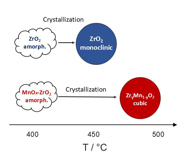
The crystallization process of MnOx–ZrO2 mixed oxide in different gas environments was studied by in situ X-ray diffraction and thermogravimetric analysis. The non-modified ZrO2 was used as a reference. The process of crystallization in Mn-containing sample dependents on the environment: the crystallization temperature in reducing and inert environment was 450 – 455 ◦C and in oxidizing it was 560 ◦C. Thus, the addition of manganese led to the shift of crystallization temperature to the higher values compared to reference sample ZrO2 (425 ◦C). The resulting crystalline phase was Zr1−yMnyO2 solid solution rather than pure zirconia. Mn cations seemed to stabilize the tetragonal zirconia instead of monoclinic.

This study presents the synthesis and characterization of composite photocatalysts based on g- C3N4 modified with Ni(OH)2 and Co(OH)2 for CO2 reduction under visible light (λ = 410 nm). XRD, UV-Vis spectroscopy, and high-resolution TEM analyses revealed that the deposition of hydroxides did not disrupt the g-C3N4 structure but caused a slight increase in the interlayer spacing and band gap; Ni(OH)2 formed nanoparticles of ∼7 nm, whereas Co(OH)2 crystallized as larger particles of ∼24 nm. TEM showed that after the photocatalytic CO2 reduction, partial agglomeration of Ni(OH)2/NiO occurs. The catalyst containing 0.1 wt.% Ni(OH)2 exhibited the highest activity – 7.04 μmol·g−1·h−1, achieving a CO2 reduction rate 1.9 times higher than that of pristine g-C3N4. The 0.5 wt.% Co(OH)2/g-C3N4 photocatalyst was achieved a 1.3-fold increase in activity compared to pristine g-C3N4. This enhancement is attributed to the formation of a II type heterojunction between g-C3N4 and Ni(OH)2, which facilitates charge transfer and suppresses recombination.
For the first time the thermal stability of the phase composition of (ZnS)(Ag2S)x sulfide heteronanostructures are studied. Solid-phase heteronanostructures (ZnS)(Ag2S)x with x = 0.002 – 0.50 are synthesized by hydrochemical co-deposition of ZnS and Ag2S sulfides. The ZnS nanoparticle size, estimated from the broadening of diffraction reflections, in the produced initial heteronanostructures is 2 – 4 nm. Annealing of the synthesized (ZnS)(Ag2S)x heteronanostructures in air at temperature from 25 to 530 ◦C and above leads to a change in their phase composition due to the oxidation of cubic ZnS sulfide to hexagonal zinc oxide. Oxidation begins at a temperature of approximately 250 ◦C; the ZnO nanoparticle size varies in a range of 12 to 17 – 25 nm. Oxidation of solid-phase (ZnS)(Ag2S)x heteronanostructures in air showed that weight loss that occurs upon heating from ∼250 to ∼430 – 450 ◦C is associated with the beginning of oxidation of the ZnS sulfide and the formation of the ZnO oxide. The most significant weight loss is observed after heating from ∼450 to ∼580 ◦C due to an increase in the ZnO content, oxidation of sulfur and its removal in the form of SO2.
The ZrB2–ZrC ceramic powders were prepared by self-propagating high-temperature synthesis (SHS) using Zr–B4C composite powders as a precursor. Composite powders were obtained by ball milling in hexane (3÷12 min). The structure, morphology, phase and fractional composition were investigated for both composite powders and SHS products. It was found that B4C grains are intensively embedded in Zr, and their distribution in composite particles becomes uniform by 9 min of ball milling. The possible route of the SHS reaction is proposed.
A comparative assessment of the influence of 2D graphene structures derived from lignin, starch and cellulose through the self-propagating high-temperature synthesis method on the mechanical, thermal and electrical properties of poly(4,4’-oxydiphenylene pyromellitimide) films was conducted. It was found that the incorporation of synthesized nanoparticles allows for the modification of the mechanical properties of the polyimide material without a significant decrease in volume and surface resistivity. Dependencies of the changes in properties of nanocomposite film materials on the following factors have also been established and analyzed: the type of biopolymer from which the nanofiller was obtained; the morphometric parameters of the prepared nanosized material; the concentration of the nanofiller.
Stability and durability of electrochemical energy conversion systems are significant issues. In this study, few-layer graphene and polytetrafluoroethylene were applied to both sides of the Nafion type membrane as barrier layers to increase the device's resistance to electrochemical exposure. Electrochemical performance was assessed in a two-electrode configuration: potentiostatic aging at 2.5 V and hydrogen crossover measurements. The characterization of materials functioning as barrier layers was conducted using scanning and transmission electron microscopy, laser correlation spectroscopy, and differential thermal analysis. It is shown that both components stabilize Nafion through interfacial interactions, resulting in a longer service life and reduced hydrogen crossover. While the reference sample showed increased crossover, the modified samples exhibited reductions of 50% and 33%. These findings underscore the potential of the studied materials in enhancing the stability of polymer electrolyte membrane water electrolyzers, contributing to the advancement of more durable and efficient systems for hydrogen energy applications.
This study presents the synthesis and characterization of composite photocatalysts based on g-C3N4 modified with Ni(OH)2 and Co(OH)2 for CO2 reduction under visible light (λ = 410 nm). XRD, UV-Vis spectroscopy, and high-resolution TEM analyses revealed that the deposition of hydroxides did not disrupt the g-C3N4 structure but caused a slight increase in the interlayer spacing and band gap; Ni(OH)2 formed nanoparticles of ~7 nm, whereas Co(OH)2 crystallized as larger particles of ~24 nm. TEM showed that after the photocatalytic CO2 reduction, partial agglomeration of Ni(OH)2/NiO occurs. The catalyst containing 0.1 wt.% Ni(OH)2 exhibited the highest activity – 7.04 μmol·g-1·h-1, achieving a CO2 reduction rate 1.9 times higher than that of pristine g-C3N4. The 0.5 wt.% Co(OH)2/g-C3N4 photocatalyst was achieved a 1.3-fold increase in activity compared to pristine g-C3N4. This enhancement is attributed to the formation of a II type heterojunction between g-C3N4 and Ni(OH)2, which facilitates charge transfer and suppresses recombination.
In this work, we report the one-pot aqueous synthesis of AuNPs using novel amidine derivatives of the closo-decaborate anion, functionalized with pendant thiol groups, as combined reducing and stabilizing agents. A comprehensive characterization using transmission electron microscopy (TEM) revealed the formation of nanoparticles with a distinctive and unusual hollow-core/dense-shell architecture, where a gold-rich shell encapsulates a low-Z element core. This unique morphology accounts for the observed absence of a characteristic surface plasmon resonance (SPR) band in the UV-Vis spectra, distinguishing these materials from classical solid-core AuNPs. X-ray photoelectron spectroscopy (XPS) confirmed the covalent attachment of the ligands via Au-S bonds and the integrity of the boron cage on the nanoparticle surface. The synthesis was optimized, establishing a 1:6 (Au:Ligand) molar ratio as ideal for achieving a narrow particle size distribution.

ISSN 2305-7971 (Online)


